Our research interests are aimed at understanding and controlling the light-matter interaction at the nanoscale in condensed matter systems. These interactions are at the core of many photonic technologies that are rapidly developing and becoming prevalent in everyday life. In the last decades, great research efforts have been devoted to the realization of high-performance and low-cost optical components that now play a key role in a wide range of applications, from city lighting to quantum information. Solid state emitters, such as excitons (bound electron-hole pairs in semiconductors) or atomic defects, form the basis of many optically active components, i.e. light sources, modulators and detectors, because they allow for scalable architectures and, at the same time, for straightforward optical manipulation.
A promising frontier of research in this field is the development of integrable non-classical light sources compatible with different platforms for on-chip logic architectures. The emerging of new two-dimensional (2D) materials promise novel functionalities, discoveries and applications in optics and electronics. These materials possess properties that were unthinkable just a decade ago, and enable to design and construct “quantum” devices directly at the atomic scale.
The goal of the lab is to combine ideas from condensed matter physics, quantum optics, and atomic physics to take advantage of the promising properties of the new 2D materials. The resulting quantum systems have the potential to open up new regimes of science in condensed matter and enable new generations of devices in areas including opto-electronics, sensing and quantum information science.
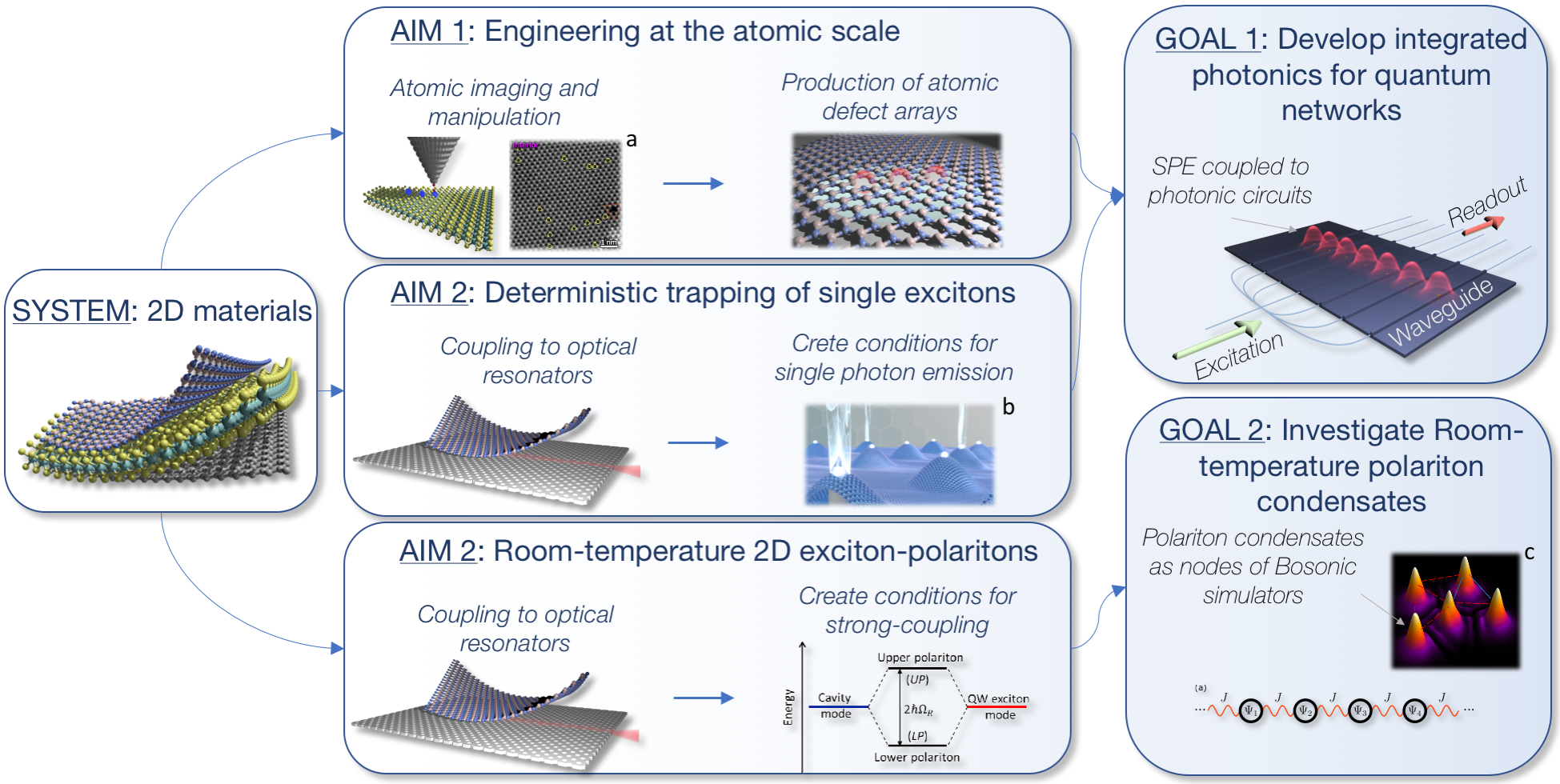
Atomic Engineering of 2D materials
Atom-like quantum emitters in solids
 have seen exceptional progress and now set the state of the art in several key quantum technologies, including single and entangled-photon emission, spin-based quantum sensors and spin-based quantum memories. However, research efforts are running up against several common key challenges: a lack of tools to produce and image solid-state quantum systems at the atomic scale; a lack of spectroscopic tools to characterize and control complex solid-state quantum systems; and an inability of theoretical tools to model quantum materials quantitatively and to predict promising new candidate systems.
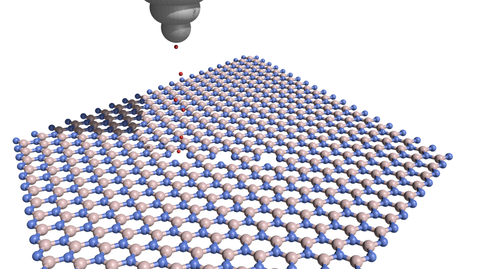
A primary focus of the lab is on patterning defects into high-quality 2D materials, used as “atomic canvases” that presents all atoms on the surface. Modern scanning electron transmission microscopes (STEM) can directly image and enable defect generation in-situ with atomic precision by controlling beam dwell time and energy.
By employing these techniques we develop arrays of high-quality atom-like quantum emitters with long spin coherence times; quantum-enhanced sensing capabilities; and photon-mediated quantum entanglement between two stable quantum emitter systems using spectrally tunable, waveguide-integrated quantum emitters.
Scalable arrays of tunable quantum emitters
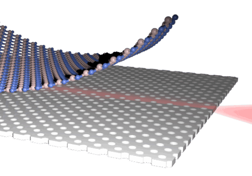
Transition metal dichalcogenides (TMDs) are 2D semiconductors at the monolayer level and have emerged as promising materials for quantum information processing with the discovery of stable quantum emitters . In this system, quantum emitters work in similar way to quantum dots in standard semiconductors with single excitons localized and bound to impurities or atomic defects that create natural potential traps. Unfortunately, the trapping sites are randomly located in the crystal lattice and no control is available on their spatial position, the trap depth and the binding energy.
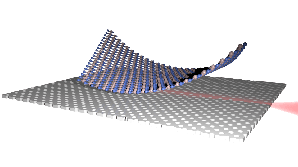
Instead of relying on random defects and impurities, our group focuses on coupling 2D TMDs to optical nano-resonators and engineer gate-tunable electrostatic traps for single excitons. The variation of the potential results in a tunable emission energy of the localized excitons and thus of the single photon emission. Van der Waals materials allow for assembly of heterogeneous structures and easy integration with more complex platforms to realize new electronic, optical, and materials functionalities.